1. Crystal Structure and Polytypism of Silicon Carbide
1.1 Cubic and Hexagonal Polytypes: From 3C to 6H and Beyond
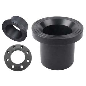
(Silicon Carbide Ceramics)
Silicon carbide (SiC) is a covalently adhered ceramic composed of silicon and carbon atoms organized in a tetrahedral coordination, forming one of one of the most complicated systems of polytypism in products scientific research.
Unlike most porcelains with a single stable crystal framework, SiC exists in over 250 recognized polytypes– distinct stacking sequences of close-packed Si-C bilayers along the c-axis– ranging from cubic 3C-SiC (additionally called β-SiC) to hexagonal 6H-SiC and rhombohedral 15R-SiC.
One of the most common polytypes used in engineering applications are 3C (cubic), 4H, and 6H (both hexagonal), each showing slightly various electronic band structures and thermal conductivities.
3C-SiC, with its zinc blende framework, has the narrowest bandgap (~ 2.3 eV) and is typically expanded on silicon substratums for semiconductor gadgets, while 4H-SiC supplies premium electron movement and is chosen for high-power electronics.
The strong covalent bonding and directional nature of the Si– C bond provide extraordinary firmness, thermal stability, and resistance to slip and chemical attack, making SiC suitable for extreme atmosphere applications.
1.2 Issues, Doping, and Electronic Residence
Despite its structural intricacy, SiC can be doped to accomplish both n-type and p-type conductivity, enabling its usage in semiconductor gadgets.
Nitrogen and phosphorus act as contributor pollutants, introducing electrons into the transmission band, while aluminum and boron work as acceptors, developing holes in the valence band.
Nonetheless, p-type doping efficiency is restricted by high activation powers, specifically in 4H-SiC, which poses difficulties for bipolar tool design.
Indigenous defects such as screw dislocations, micropipes, and piling faults can deteriorate tool performance by serving as recombination facilities or leak courses, necessitating top notch single-crystal growth for electronic applications.
The large bandgap (2.3– 3.3 eV depending on polytype), high break down electric area (~ 3 MV/cm), and superb thermal conductivity (~ 3– 4 W/m · K for 4H-SiC) make SiC far above silicon in high-temperature, high-voltage, and high-frequency power electronics.
2. Processing and Microstructural Engineering
( Silicon Carbide Ceramics)
2.1 Sintering and Densification Methods
Silicon carbide is naturally hard to densify as a result of its strong covalent bonding and reduced self-diffusion coefficients, needing advanced processing approaches to accomplish complete density without additives or with marginal sintering help.
Pressureless sintering of submicron SiC powders is possible with the addition of boron and carbon, which advertise densification by eliminating oxide layers and improving solid-state diffusion.
Warm pushing applies uniaxial stress during home heating, allowing complete densification at reduced temperature levels (~ 1800– 2000 ° C )and producing fine-grained, high-strength elements ideal for reducing tools and use components.
For big or complex shapes, reaction bonding is utilized, where porous carbon preforms are infiltrated with liquified silicon at ~ 1600 ° C, developing β-SiC sitting with marginal contraction.
Nonetheless, recurring cost-free silicon (~ 5– 10%) continues to be in the microstructure, limiting high-temperature efficiency and oxidation resistance over 1300 ° C.
2.2 Additive Production and Near-Net-Shape Manufacture
Current developments in additive manufacturing (AM), especially binder jetting and stereolithography using SiC powders or preceramic polymers, allow the construction of complicated geometries formerly unattainable with standard techniques.
In polymer-derived ceramic (PDC) paths, liquid SiC precursors are shaped using 3D printing and after that pyrolyzed at heats to generate amorphous or nanocrystalline SiC, typically calling for additional densification.
These methods decrease machining expenses and material waste, making SiC a lot more obtainable for aerospace, nuclear, and warmth exchanger applications where complex styles improve performance.
Post-processing steps such as chemical vapor seepage (CVI) or liquid silicon seepage (LSI) are sometimes made use of to improve density and mechanical honesty.
3. Mechanical, Thermal, and Environmental Performance
3.1 Strength, Solidity, and Use Resistance
Silicon carbide rates among the hardest recognized materials, with a Mohs solidity of ~ 9.5 and Vickers firmness going beyond 25 Grade point average, making it very resistant to abrasion, erosion, and damaging.
Its flexural stamina normally varies from 300 to 600 MPa, depending upon handling approach and grain size, and it preserves strength at temperature levels as much as 1400 ° C in inert atmospheres.
Fracture durability, while moderate (~ 3– 4 MPa · m ONE/ TWO), is sufficient for many structural applications, especially when incorporated with fiber support in ceramic matrix compounds (CMCs).
SiC-based CMCs are utilized in wind turbine blades, combustor linings, and brake systems, where they supply weight savings, fuel effectiveness, and expanded service life over metal equivalents.
Its excellent wear resistance makes SiC perfect for seals, bearings, pump components, and ballistic shield, where toughness under severe mechanical loading is important.
3.2 Thermal Conductivity and Oxidation Security
One of SiC’s most useful residential properties is its high thermal conductivity– as much as 490 W/m · K for single-crystal 4H-SiC and ~ 30– 120 W/m · K for polycrystalline types– going beyond that of numerous metals and making it possible for reliable warm dissipation.
This residential or commercial property is crucial in power electronics, where SiC devices produce much less waste warmth and can operate at higher power thickness than silicon-based gadgets.
At elevated temperature levels in oxidizing settings, SiC creates a protective silica (SiO ₂) layer that slows down more oxidation, providing excellent environmental sturdiness up to ~ 1600 ° C.
Nonetheless, in water vapor-rich environments, this layer can volatilize as Si(OH)₄, bring about increased degradation– a vital difficulty in gas turbine applications.
4. Advanced Applications in Power, Electronics, and Aerospace
4.1 Power Electronics and Semiconductor Instruments
Silicon carbide has actually changed power electronic devices by making it possible for devices such as Schottky diodes, MOSFETs, and JFETs that run at higher voltages, frequencies, and temperature levels than silicon matchings.
These tools reduce power losses in electric lorries, renewable resource inverters, and industrial motor drives, adding to worldwide power effectiveness enhancements.
The ability to run at joint temperature levels above 200 ° C enables streamlined air conditioning systems and increased system dependability.
Moreover, SiC wafers are made use of as substrates for gallium nitride (GaN) epitaxy in high-electron-mobility transistors (HEMTs), integrating the benefits of both wide-bandgap semiconductors.
4.2 Nuclear, Aerospace, and Optical Systems
In atomic power plants, SiC is a vital element of accident-tolerant fuel cladding, where its low neutron absorption cross-section, radiation resistance, and high-temperature toughness boost safety and efficiency.
In aerospace, SiC fiber-reinforced compounds are utilized in jet engines and hypersonic cars for their light-weight and thermal security.
Additionally, ultra-smooth SiC mirrors are utilized precede telescopes due to their high stiffness-to-density ratio, thermal stability, and polishability to sub-nanometer roughness.
In summary, silicon carbide ceramics represent a keystone of modern-day advanced products, combining exceptional mechanical, thermal, and electronic residential properties.
Through specific control of polytype, microstructure, and processing, SiC continues to make it possible for technological innovations in energy, transport, and severe atmosphere engineering.
5. Vendor
TRUNNANO is a supplier of Spherical Tungsten Powder with over 12 years of experience in nano-building energy conservation and nanotechnology development. It accepts payment via Credit Card, T/T, West Union and Paypal. Trunnano will ship the goods to customers overseas through FedEx, DHL, by air, or by sea. If you want to know more about Spherical Tungsten Powder, please feel free to contact us and send an inquiry(sales5@nanotrun.com).
Tags: silicon carbide ceramic,silicon carbide ceramic products, industry ceramic
All articles and pictures are from the Internet. If there are any copyright issues, please contact us in time to delete.
Inquiry us