1. Material Principles and Structural Features of Alumina Ceramics
1.1 Crystallographic and Compositional Basis of α-Alumina
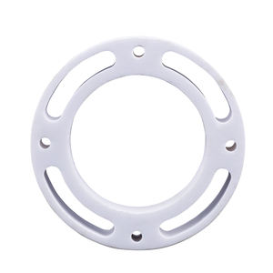
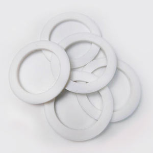
(Alumina Ceramic Substrates)
Alumina ceramic substrates, mostly made up of aluminum oxide (Al ₂ O FOUR), act as the foundation of contemporary digital packaging due to their remarkable balance of electrical insulation, thermal security, mechanical strength, and manufacturability.
The most thermodynamically secure stage of alumina at high temperatures is corundum, or α-Al Two O SIX, which crystallizes in a hexagonal close-packed oxygen latticework with aluminum ions occupying two-thirds of the octahedral interstitial websites.
This thick atomic setup imparts high firmness (Mohs 9), outstanding wear resistance, and strong chemical inertness, making α-alumina appropriate for extreme operating settings.
Business substratums usually consist of 90– 99.8% Al Two O FIVE, with small enhancements of silica (SiO ₂), magnesia (MgO), or rare earth oxides utilized as sintering help to promote densification and control grain development throughout high-temperature handling.
Greater pureness qualities (e.g., 99.5% and above) display exceptional electric resistivity and thermal conductivity, while lower pureness variations (90– 96%) provide affordable services for much less demanding applications.
1.2 Microstructure and Flaw Design for Electronic Integrity
The efficiency of alumina substrates in electronic systems is seriously depending on microstructural uniformity and problem minimization.
A penalty, equiaxed grain structure– normally varying from 1 to 10 micrometers– guarantees mechanical stability and decreases the likelihood of fracture proliferation under thermal or mechanical anxiety.
Porosity, specifically interconnected or surface-connected pores, have to be decreased as it breaks down both mechanical strength and dielectric efficiency.
Advanced handling techniques such as tape spreading, isostatic pushing, and controlled sintering in air or controlled environments enable the production of substratums with near-theoretical thickness (> 99.5%) and surface area roughness listed below 0.5 µm, important for thin-film metallization and cable bonding.
In addition, contamination partition at grain boundaries can lead to leakage currents or electrochemical migration under prejudice, necessitating rigorous control over raw material purity and sintering problems to make sure long-term dependability in humid or high-voltage settings.
2. Manufacturing Processes and Substrate Fabrication Technologies
( Alumina Ceramic Substrates)
2.1 Tape Casting and Green Body Processing
The production of alumina ceramic substratums starts with the preparation of an extremely spread slurry consisting of submicron Al two O two powder, natural binders, plasticizers, dispersants, and solvents.
This slurry is processed using tape spreading– a continual approach where the suspension is spread over a moving provider movie making use of an accuracy physician blade to achieve consistent thickness, generally between 0.1 mm and 1.0 mm.
After solvent dissipation, the resulting “eco-friendly tape” is versatile and can be punched, drilled, or laser-cut to create using openings for upright affiliations.
Numerous layers may be laminated to produce multilayer substrates for intricate circuit assimilation, although the majority of industrial applications utilize single-layer setups as a result of cost and thermal expansion considerations.
The eco-friendly tapes are after that thoroughly debound to eliminate natural ingredients through controlled thermal decomposition prior to last sintering.
2.2 Sintering and Metallization for Circuit Assimilation
Sintering is carried out in air at temperature levels between 1550 ° C and 1650 ° C, where solid-state diffusion drives pore elimination and grain coarsening to achieve complete densification.
The direct contraction throughout sintering– typically 15– 20%– have to be precisely predicted and made up for in the layout of eco-friendly tapes to ensure dimensional precision of the final substrate.
Complying with sintering, metallization is applied to develop conductive traces, pads, and vias.
Two main approaches dominate: thick-film printing and thin-film deposition.
In thick-film technology, pastes having steel powders (e.g., tungsten, molybdenum, or silver-palladium alloys) are screen-printed onto the substratum and co-fired in a minimizing ambience to form durable, high-adhesion conductors.
For high-density or high-frequency applications, thin-film procedures such as sputtering or dissipation are used to deposit bond layers (e.g., titanium or chromium) adhered to by copper or gold, allowing sub-micron patterning via photolithography.
Vias are full of conductive pastes and discharged to develop electrical interconnections in between layers in multilayer styles.
3. Functional Features and Efficiency Metrics in Electronic Equipment
3.1 Thermal and Electric Actions Under Operational Stress And Anxiety
Alumina substratums are prized for their favorable combination of moderate thermal conductivity (20– 35 W/m · K for 96– 99.8% Al Two O FOUR), which makes it possible for effective warmth dissipation from power tools, and high volume resistivity (> 10 ¹⁴ Ω · centimeters), making certain very little leakage current.
Their dielectric constant (εᵣ ≈ 9– 10 at 1 MHz) is secure over a wide temperature level and regularity range, making them appropriate for high-frequency circuits up to a number of ghzs, although lower-κ materials like aluminum nitride are preferred for mm-wave applications.
The coefficient of thermal expansion (CTE) of alumina (~ 6.8– 7.2 ppm/K) is sensibly well-matched to that of silicon (~ 3 ppm/K) and specific packaging alloys, minimizing thermo-mechanical anxiety during gadget operation and thermal cycling.
Nonetheless, the CTE inequality with silicon stays a worry in flip-chip and direct die-attach setups, commonly requiring certified interposers or underfill products to minimize exhaustion failure.
3.2 Mechanical Toughness and Ecological Resilience
Mechanically, alumina substratums show high flexural strength (300– 400 MPa) and excellent dimensional stability under lots, allowing their usage in ruggedized electronic devices for aerospace, vehicle, and industrial control systems.
They are immune to resonance, shock, and creep at elevated temperature levels, maintaining architectural honesty as much as 1500 ° C in inert atmospheres.
In moist settings, high-purity alumina reveals marginal wetness absorption and excellent resistance to ion migration, making certain long-lasting dependability in exterior and high-humidity applications.
Surface hardness also protects against mechanical damages throughout handling and setting up, although care needs to be required to stay clear of edge damaging because of inherent brittleness.
4. Industrial Applications and Technical Effect Throughout Sectors
4.1 Power Electronic Devices, RF Modules, and Automotive Systems
Alumina ceramic substrates are common in power digital components, including insulated gate bipolar transistors (IGBTs), MOSFETs, and rectifiers, where they give electric seclusion while assisting in warmth transfer to warm sinks.
In radio frequency (RF) and microwave circuits, they work as provider systems for hybrid integrated circuits (HICs), surface acoustic wave (SAW) filters, and antenna feed networks due to their steady dielectric buildings and low loss tangent.
In the automotive sector, alumina substratums are used in engine control units (ECUs), sensing unit bundles, and electric lorry (EV) power converters, where they withstand heats, thermal biking, and direct exposure to corrosive fluids.
Their reliability under severe problems makes them vital for safety-critical systems such as anti-lock stopping (ABDOMINAL) and progressed vehicle driver support systems (ADAS).
4.2 Medical Gadgets, Aerospace, and Arising Micro-Electro-Mechanical Systems
Beyond customer and industrial electronic devices, alumina substratums are used in implantable medical devices such as pacemakers and neurostimulators, where hermetic securing and biocompatibility are extremely important.
In aerospace and protection, they are utilized in avionics, radar systems, and satellite interaction components as a result of their radiation resistance and stability in vacuum cleaner environments.
Moreover, alumina is significantly used as a structural and protecting platform in micro-electro-mechanical systems (MEMS), consisting of pressure sensing units, accelerometers, and microfluidic tools, where its chemical inertness and compatibility with thin-film handling are beneficial.
As digital systems remain to demand greater power densities, miniaturization, and reliability under severe conditions, alumina ceramic substrates stay a cornerstone material, linking the void in between efficiency, price, and manufacturability in advanced electronic product packaging.
5. Supplier
Alumina Technology Co., Ltd focus on the research and development, production and sales of aluminum oxide powder, aluminum oxide products, aluminum oxide crucible, etc., serving the electronics, ceramics, chemical and other industries. Since its establishment in 2005, the company has been committed to providing customers with the best products and services. If you are looking for high quality b alumina, please feel free to contact us. (nanotrun@yahoo.com)
Tags: Alumina Ceramic Substrates, Alumina Ceramics, alumina
All articles and pictures are from the Internet. If there are any copyright issues, please contact us in time to delete.
Inquiry us