1. Fundamental Framework and Polymorphism of Silicon Carbide
1.1 Crystal Chemistry and Polytypic Variety
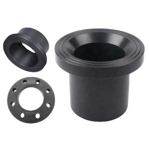
(Silicon Carbide Ceramics)
Silicon carbide (SiC) is a covalently adhered ceramic material made up of silicon and carbon atoms set up in a tetrahedral coordination, forming a very stable and robust crystal latticework.
Unlike several standard porcelains, SiC does not possess a single, one-of-a-kind crystal structure; instead, it exhibits an amazing phenomenon known as polytypism, where the exact same chemical composition can take shape into over 250 distinctive polytypes, each differing in the stacking series of close-packed atomic layers.
One of the most technologically substantial polytypes are 3C-SiC (cubic, zinc blende structure), 4H-SiC, and 6H-SiC (both hexagonal), each offering various electronic, thermal, and mechanical buildings.
3C-SiC, likewise referred to as beta-SiC, is commonly formed at lower temperature levels and is metastable, while 4H and 6H polytypes, referred to as alpha-SiC, are a lot more thermally steady and generally utilized in high-temperature and electronic applications.
This architectural diversity enables targeted material option based on the designated application, whether it be in power electronic devices, high-speed machining, or extreme thermal settings.
1.2 Bonding Features and Resulting Feature
The stamina of SiC comes from its solid covalent Si-C bonds, which are short in size and extremely directional, causing a rigid three-dimensional network.
This bonding arrangement imparts phenomenal mechanical homes, consisting of high hardness (typically 25– 30 Grade point average on the Vickers range), exceptional flexural stamina (as much as 600 MPa for sintered kinds), and good fracture toughness relative to various other porcelains.
The covalent nature additionally adds to SiC’s exceptional thermal conductivity, which can reach 120– 490 W/m · K depending on the polytype and pureness– similar to some steels and much going beyond most architectural porcelains.
In addition, SiC displays a low coefficient of thermal development, around 4.0– 5.6 × 10 ⁻⁶/ K, which, when incorporated with high thermal conductivity, provides it outstanding thermal shock resistance.
This suggests SiC parts can go through rapid temperature adjustments without breaking, an important feature in applications such as heating system components, heat exchangers, and aerospace thermal defense systems.
2. Synthesis and Processing Strategies for Silicon Carbide Ceramics
( Silicon Carbide Ceramics)
2.1 Primary Manufacturing Methods: From Acheson to Advanced Synthesis
The industrial manufacturing of silicon carbide dates back to the late 19th century with the invention of the Acheson process, a carbothermal decrease method in which high-purity silica (SiO ₂) and carbon (generally oil coke) are heated up to temperatures over 2200 ° C in an electrical resistance heating system.
While this approach continues to be extensively used for generating rugged SiC powder for abrasives and refractories, it produces product with pollutants and irregular fragment morphology, restricting its usage in high-performance porcelains.
Modern improvements have brought about alternative synthesis paths such as chemical vapor deposition (CVD), which creates ultra-high-purity, single-crystal SiC for semiconductor applications, and laser-assisted or plasma-enhanced synthesis for nanoscale powders.
These advanced techniques make it possible for specific control over stoichiometry, bit size, and phase purity, vital for customizing SiC to specific design demands.
2.2 Densification and Microstructural Control
Among the greatest difficulties in producing SiC ceramics is attaining complete densification as a result of its solid covalent bonding and reduced self-diffusion coefficients, which prevent conventional sintering.
To conquer this, numerous customized densification techniques have been developed.
Reaction bonding involves infiltrating a porous carbon preform with molten silicon, which responds to create SiC in situ, causing a near-net-shape part with very little contraction.
Pressureless sintering is accomplished by including sintering help such as boron and carbon, which promote grain border diffusion and remove pores.
Warm pushing and hot isostatic pressing (HIP) use exterior pressure during heating, enabling full densification at lower temperature levels and producing products with superior mechanical buildings.
These processing methods allow the fabrication of SiC elements with fine-grained, uniform microstructures, vital for maximizing toughness, wear resistance, and dependability.
3. Functional Efficiency and Multifunctional Applications
3.1 Thermal and Mechanical Durability in Extreme Atmospheres
Silicon carbide porcelains are uniquely fit for operation in extreme problems as a result of their capacity to keep architectural integrity at high temperatures, withstand oxidation, and endure mechanical wear.
In oxidizing ambiences, SiC develops a protective silica (SiO TWO) layer on its surface, which slows down additional oxidation and permits continual usage at temperature levels up to 1600 ° C.
This oxidation resistance, integrated with high creep resistance, makes SiC suitable for elements in gas turbines, combustion chambers, and high-efficiency warmth exchangers.
Its extraordinary firmness and abrasion resistance are made use of in commercial applications such as slurry pump components, sandblasting nozzles, and reducing tools, where metal alternatives would swiftly weaken.
Moreover, SiC’s low thermal growth and high thermal conductivity make it a preferred material for mirrors precede telescopes and laser systems, where dimensional stability under thermal cycling is paramount.
3.2 Electrical and Semiconductor Applications
Beyond its architectural utility, silicon carbide plays a transformative function in the area of power electronic devices.
4H-SiC, particularly, possesses a large bandgap of around 3.2 eV, making it possible for tools to operate at greater voltages, temperatures, and changing regularities than standard silicon-based semiconductors.
This leads to power devices– such as Schottky diodes, MOSFETs, and JFETs– with considerably reduced power losses, smaller sized dimension, and improved efficiency, which are currently extensively utilized in electrical automobiles, renewable resource inverters, and wise grid systems.
The high break down electrical area of SiC (about 10 times that of silicon) permits thinner drift layers, lowering on-resistance and improving device performance.
Additionally, SiC’s high thermal conductivity helps dissipate warm effectively, lowering the need for large cooling systems and enabling even more small, reputable electronic modules.
4. Arising Frontiers and Future Expectation in Silicon Carbide Technology
4.1 Assimilation in Advanced Power and Aerospace Equipments
The ongoing transition to tidy power and amazed transport is driving unprecedented demand for SiC-based elements.
In solar inverters, wind power converters, and battery management systems, SiC devices contribute to greater power conversion performance, straight lowering carbon exhausts and functional costs.
In aerospace, SiC fiber-reinforced SiC matrix composites (SiC/SiC CMCs) are being created for turbine blades, combustor liners, and thermal security systems, providing weight savings and efficiency gains over nickel-based superalloys.
These ceramic matrix composites can operate at temperature levels surpassing 1200 ° C, enabling next-generation jet engines with higher thrust-to-weight proportions and boosted fuel efficiency.
4.2 Nanotechnology and Quantum Applications
At the nanoscale, silicon carbide displays one-of-a-kind quantum homes that are being explored for next-generation innovations.
Particular polytypes of SiC host silicon jobs and divacancies that function as spin-active problems, operating as quantum little bits (qubits) for quantum computer and quantum noticing applications.
These flaws can be optically booted up, adjusted, and read out at space temperature level, a significant advantage over several other quantum platforms that require cryogenic problems.
Furthermore, SiC nanowires and nanoparticles are being checked out for usage in area discharge gadgets, photocatalysis, and biomedical imaging because of their high facet ratio, chemical stability, and tunable digital residential or commercial properties.
As study progresses, the integration of SiC into crossbreed quantum systems and nanoelectromechanical tools (NEMS) promises to increase its duty beyond traditional engineering domains.
4.3 Sustainability and Lifecycle Factors To Consider
The manufacturing of SiC is energy-intensive, specifically in high-temperature synthesis and sintering procedures.
However, the lasting advantages of SiC components– such as extended life span, reduced maintenance, and boosted system performance– typically outweigh the first environmental footprint.
Efforts are underway to establish more lasting manufacturing routes, including microwave-assisted sintering, additive manufacturing (3D printing) of SiC, and recycling of SiC waste from semiconductor wafer processing.
These advancements intend to lower energy usage, lessen product waste, and sustain the round economy in innovative products sectors.
In conclusion, silicon carbide porcelains represent a foundation of modern materials scientific research, connecting the space in between structural toughness and functional adaptability.
From enabling cleaner power systems to powering quantum innovations, SiC continues to redefine the limits of what is feasible in design and science.
As processing strategies advance and brand-new applications emerge, the future of silicon carbide stays incredibly bright.
5. Supplier
Advanced Ceramics founded on October 17, 2012, is a high-tech enterprise committed to the research and development, production, processing, sales and technical services of ceramic relative materials and products. Our products includes but not limited to Boron Carbide Ceramic Products, Boron Nitride Ceramic Products, Silicon Carbide Ceramic Products, Silicon Nitride Ceramic Products, Zirconium Dioxide Ceramic Products, etc. If you are interested, please feel free to contact us.(nanotrun@yahoo.com)
Tags: Silicon Carbide Ceramics,silicon carbide,silicon carbide price
All articles and pictures are from the Internet. If there are any copyright issues, please contact us in time to delete.
Inquiry us